Angle-Resolved Photoemission Spectroscopy

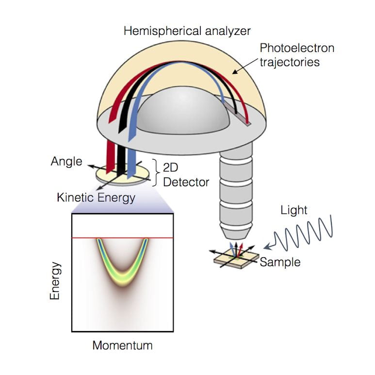
In solid state systems, electrons form electronic band structures in the energy-momentum space. These band structures are the basis for macroscopic electronic and optical properties such as electrical transport, heat transport, and certain types of magnetism. Angle-resolved photoemission spectroscopy (ARPES) is a powerful tool to directly measure the electronic band structure. The principle of ARPES is based on the photoelectric effect, which was first explained by Albert Einstein. A light beam with a photon energy higher than the material’s work function is incident on the sample in an ultrahigh vacuum environment (<1e-10 Torr). Photoelectrons are generated and collected by a hemispherical analyzer. The analyzer resolves the emission angle and the kinetic energy of the photoelectrons. Based on the conservation laws of energy and momentum, one can re-construct the electronic binding energy as a function of crystal momentum, which is precisely the electronic band structure.
More precisely, ARPES measures the “single-particle spectral function,” which encodes not only the band structure but also the electronic interactions. Therefore, using ARPES we understand the fundamental electronic interactions in a solid, and can relate to collective quantum phenomena such as superconductivity, charge order, and topological phases. In our lab, we connect MBE with an in situ ARPES setup, which enables a positive feedback loop for scientific investigation: MBE produces novel materials for ARPES studies; ARPES provides instant understanding which is crucial for MBE synthesis.
Time-Resolved ARPES

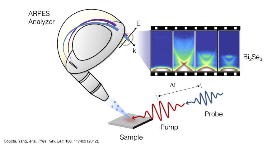
A recent advance in ARPES technologies is femtosecond time-resolved ARPES (trARPES). Dr. Yang was one of the core people developing this technology during his Ph.D. study. In trARPES, we combine ultrafast pump-probe spectroscopy with ARPES spectrometers. An infrared femtosecond pulse serves as the pump, which excites the electrons into excited states; an ultraviolet pulse serves as the probe, which kicks out photoelectrons to generate a photoemission spectrum. A series of spectra are generated for different pump-probe delays, which compose a movie of electrons in the energy-momentum space. This movie of electrons is vital in understanding the dynamical processes in a solid, and also provides access to nonequilibrium phenomena only in the transient state. Examples include light-induced Dirac state and light-induced Floquet states in a topological insulator. Recently, Dr. Yang utilized this technique to launch a coherent phonon oscillation in FeSe thin film superconductors, which defined a novel way of characterizing electron-phonon coupling in the time domain.
Our multi-resolution photoemission spectroscopy setup is fully commissioned, integrating traditional helium-lamp-based ARPES, ultrahigh resolution laser-ARPES, time-resolved ARPES, and μARPES. We achieve a time resolution < 35 fs in trARPES, a spatial resolution < 10 microns in μARPES, and an energy resolution < 4 meV in ultrahigh resolution laser-ARPES.
Molecular Beam Epitaxy

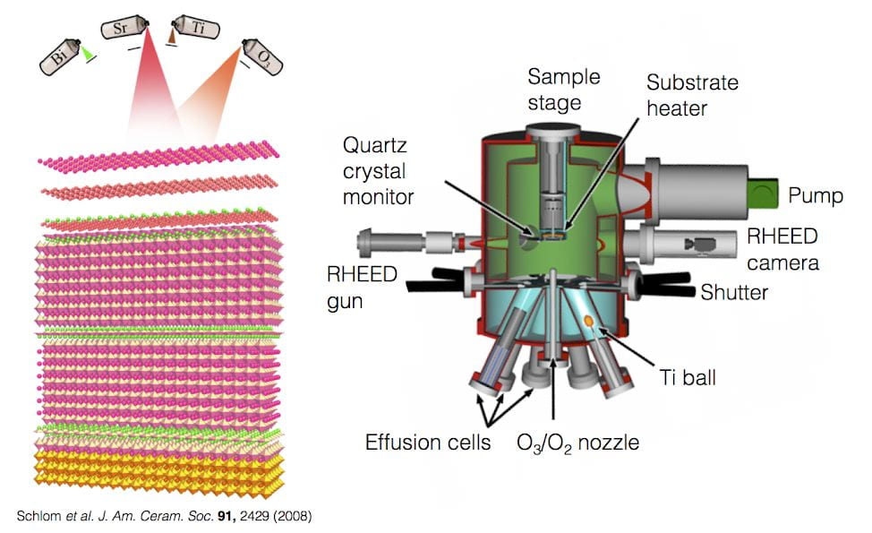
Molecular beam epitaxy (MBE) is a method of making artificial thin-film materials. Source materials are heated in effusion cells or electron-beam evaporators, and generate molecular beams shooting at the substrate for reactions. All depositions are done in an ultrahigh vacuum environment with a pressure <1e-9 Torr. This way of making materials can be regarded as “atomic painting,” where materials are made layer-by-layer with superb precision. In situ characterization tools such as quartz crystal monitor and reflection high-energy electron diffraction enable scientists to monitor the flux of sources and characterize the quality of thin films during growth. MBE has been successfully utilized to grow high quality oxides and chalcogenides. In the Yang lab, we are interested in engineering material interfaces between oxides and chalcogenides, where emergent phenomena such as superconductivity and topological orders can emerge. Building and understanding these interfaces will be the first step towards making artificial functional materials, in which electronic properties are dictated by macroscopic quantum phenomena.
